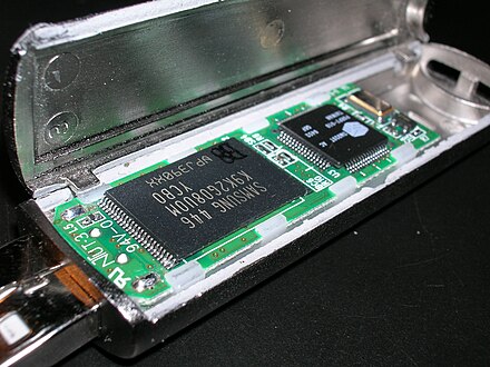
Flash memory is an electronic non-volatile computer memory storage medium that can be electrically erased and reprogrammed. The two main types of flash memory, NOR flash and NAND flash, are named for the NOR and NAND logic gates. Both use the same cell design, consisting of floating gate MOSFETs. They differ at the circuit level depending on whether the state of the bit line or word lines is pulled high or low: in NAND flash, the relationship between the bit line and the word lines resembles a NAND gate; in NOR flash, it resembles a NOR gate.
Flash memory, a type of floating-gate memory, was invented by Fujio Masuoka at Toshiba in 1980 and is based on EEPROM technology. Toshiba began marketing flash memory in 1987.[1] EPROMs had to be erased completely before they could be rewritten. NAND flash memory, however, may be erased, written, and read in blocks (or pages), which generally are much smaller than the entire device. NOR flash memory allows a single machine word to be written – to an erased location – or read independently. A flash memory device typically consists of one or more flash memory chips (each holding many flash memory cells), along with a separate flash memory controller chip.
The NAND type is found mainly in memory cards, USB flash drives, solid-state drives (those produced since 2009), feature phones, smartphones, and similar products, for general storage and transfer of data. NAND or NOR flash memory is also often used to store configuration data in digital products, a task previously made possible by EEPROM or battery-powered static RAM. A key disadvantage of flash memory is that it can endure only a relatively small number of write cycles in a specific block.[2]
NOR flash is known for its direct random access capabilities, making it apt for executing code directly. Its architecture allows for individual byte access, facilitating faster read speeds compared to NAND flash. NAND flash memory operates with a different architecture, relying on a serial access approach. This makes NAND suitable for high-density data storage but less efficient for random access tasks. NAND flash is often employed in scenarios where cost-effective, high-capacity storage is crucial, such as in USB drives, memory cards, and solid-state drives (SSDs).
The primary differentiator lies in their use cases and internal structures. NOR flash is optimal for applications requiring quick access to individual bytes, like in embedded systems for program execution. NAND flash, on the other hand, shines in scenarios demanding cost-effective, high-capacity storage with sequential data access.
Flash memory[3] is used in computers, PDAs, digital audio players, digital cameras, mobile phones, synthesizers, video games, scientific instrumentation, industrial robotics, and medical electronics. Flash memory has a fast read access time but it is not as fast as static RAM or ROM. In portable devices, it is preferred to use flash memory because of its mechanical shock resistance since mechanical drives are more prone to mechanical damage.[4]
Because erase cycles are slow, the large block sizes used in flash memory erasing give it a significant speed advantage over non-flash EEPROM when writing large amounts of data. As of 2019,[update] flash memory costs greatly less than byte-programmable EEPROM and had become the dominant memory type wherever a system required a significant amount of non-volatile solid-state storage. EEPROMs, however, are still used in applications that require only small amounts of storage, as in serial presence detect.[5][6]
Flash memory packages can use die stacking with through-silicon vias and several dozen layers of 3D TLC NAND cells (per die) simultaneously to achieve capacities of up to 1 tebibyte per package using 16 stacked dies and an integrated flash controller as a separate die inside the package.[7][8][9][10]
The origins of flash memory can be traced back to the development of the floating-gate MOSFET (FGMOS), also known as the floating-gate transistor.[11][12] The original MOSFET was invented at Bell Labs between 1955 and 1960, after Frosch and Derick discovered surface passivation and used their discovery to create the first planar transistors.[13][14][15][16][17][18] Dawon Kahng went on to develop a variation, the floating-gate MOSFET, with Taiwanese-American engineer Simon Min Sze at Bell Labs in 1967.[19] They proposed that it could be used as floating-gate memory cells for storing a form of programmable read-only memory (PROM) that is both non-volatile and re-programmable.[19]
Early types of floating-gate memory included EPROM (erasable PROM) and EEPROM (electrically erasable PROM) in the 1970s.[19] However, early floating-gate memory required engineers to build a memory cell for each bit of data, which proved to be cumbersome,[20] slow,[21] and expensive, restricting floating-gate memory to niche applications in the 1970s, such as military equipment and the earliest experimental mobile phones.[11]
Modern EEPROM based on Fowler-Nordheim tunnelling to erase data was invented by Bernward and patented by Siemens in 1974.[22] And further developed between 1976 and 1978 by Eliyahou Harari at Hughes Aircraft Company and George Perlegos and others at Intel.[23][24] This led to Masuoka's invention of flash memory at Toshiba in 1980.[20][25][26] The improvement between EEPROM and flash being that flash is programmed in blocks while EEPROM is programmed in bytes. According to Toshiba, the name "flash" was suggested by Masuoka's colleague, Shōji Ariizumi, because the erasure process of the memory contents reminded him of the flash of a camera.[27] Masuoka and colleagues presented the invention of NOR flash in 1984,[28][29] and then NAND flash at the IEEE 1987 International Electron Devices Meeting (IEDM) held in San Francisco.[30]
Toshiba commercially launched NAND flash memory in 1987.